
Precision Optics and Optoelectronics
Solution
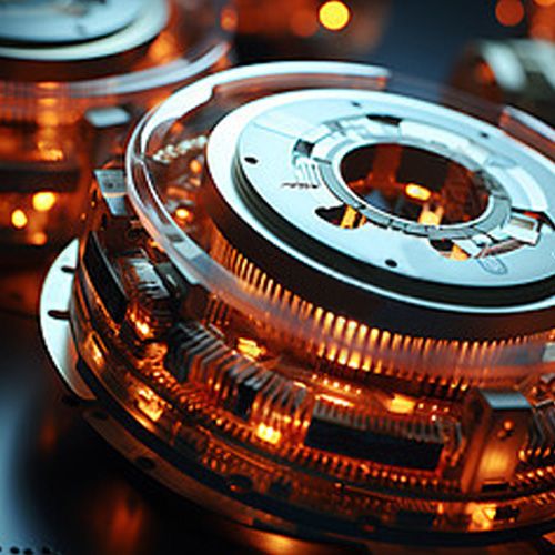
Molecular-Level Cleanliness System for Precision Optics &Optoelectronics, Protecting Surfaces, Coatings, and Performance from Nanoscale Contaminants in Imaging, Laser, and Sensor Systems
5/5
bupclean
One-stop industry service
15 years experience
Precision Optics and Optoelectronics Solutions
| Component & Typical Contaminant | Critical Need | Recommended Product | Key Rationale & Cleaning Protocol |
|---|---|---|---|
| 1. High-Value Lenses & Windows (Bare glass, AR-coated. Dust, light fingerprints) | Zero scratch risk Maximum particle removal | BN.11040324 (Ultra-Soft) | Why: Lowest dry weight (18.7g) for supreme softness; highest inherent cleanliness. Protocol: 1. Gross Clean: Use dry, gentle radial wipe (center out). 2. Solvent Clean: Lightly moisten with optic-grade acetone; use single, overlapping spiral wipe. 3. Dry Buff: Immediate buff with a third, dry wipe to prevent streaks. |
| 2. Laser Optics & Crystals (HR mirrors, Nd:YAG rods. Molecular films, dust) | Ultra-low residue (NVR) High LIDT compatibility No static charge | BN.11050135 (Low-Residue) BN.11050805 (ESD-Safe) | Why: BN.11050135: Certified low extractables for LIDT. BN.11050805: Prevents static attraction. Protocol: 1. Static Control: Dry clean with grounded BN.11050805. 2. Solvent Rinse: Flood optic with high-purity solvent. 3. Contact Clean: Gently drag solvent-saturated BN.11050135 across surface (no rubbing). 4. Dry: Air-dry vertically in clean airflow. |
| 3. Imaging Sensors & Fiber Endfaces (CCD/CMOS, fiber optics. Micro-dust, oils) | Absolute zero lint Precision form factor ESD safety | Specialized Swabs (BN-SWAB-100) BN.11050805 (perimeter) | Why: Swabs offer controlled, point-contact cleaning; material is lint-free and ESD-safe. Protocol (Fiber): 1. Inspect with scope. 2. Clean with dry swab (single-direction rotation). 3. Clean with solvent-saturated swab (IPA). 4. Final inspect. Protocol (Sensor): Use BN.11050805 for housing; swabs only for active pixel area. |
| 4. Assembly & Housing Interiors (Lens barrels, housings. Dust, handling debris) | Effective particle removal Good conformability Cost-effectiveness | BN.11050201 (Lightweight) or BN.11050207 (Balanced) | Why: Excellent cleanliness at responsible cost for non-critical surfaces. BN.11050201 is softer for sensitive finishes. Protocol: 1. Fold wipe to create clean pad. 2. Use with mild, compatible solvent. 3. Employ “rolling” motion for fresh surface contact each pass. |
Company Partners


Reliable Guarantee Customer case feedback

4.9/5
Dr. Rachel Haldims
Solving a 5nm wafer defect problem
Surface charge decreased from 250V to <50V, and defect rate decreased from 12% to 1.8%.

5/5
Dr. Mariel Senry
Static electricity damage and lint can cause short circuits.
The electrostatic discharge (ESD) failure rate decreased from 8% to 0.6%, and the short circuit rate decreased from 5% to 0.3%.

4.8/5
Dr. Damian Pix
Optical equipment lens maintenance
No new scratches, charge maintained at <30V for over 8 hours, and imaging resolution improved by 15%.

4.5/5
Dr. Shi Yon
Wafer surface particulate contamination
The surface particulate contamination rate of wafers decreased by 70%, and the overall yield increased by 5%.
Microfiber cleanroom cloth
In the nanoscale world of semiconductor manufacturing, contamination control is not an option, but a necessity. Our microfiber cleanroom wipes, designed specifically for global semiconductor front-end manufacturing and precision back-end assembly, serve as a line of defense against particulate contamination, protecting sensitive circuitry and ensuring the highest product yields. Each wipe originates from our certified ISO Class 4 core production environment, manufactured and tested according to the most stringent IEST standards, and is committed to meeting the demanding requirements from mature processes to state-of-the-art packaging technologies such as 3D-ICs.
What makes your microfiber wipers specifically suitable for Class 1 and Class 10 cleanrooms in semiconductor fabs?
Our microfiber wipers are engineered for the most critical environments. The key is our continuous filament, 100% polyester microfiber construction which is inherently low-linting. Combined with our proprietary laser-sealing edge technology, we virtually eliminate edge shedding. Each batch is validated to release < 5 particles (>0.5µm) per square foot according to IEST-RP-CC004.3, making them ideal for photolithography, wafer inspection, and sensitive assembly areas.
We experience issues with solvent absorption and residue when cleaning precision parts. How does your product address this?
Our microfiber is designed for high absorbency with low NVR (Non-Volatile Residue). The split-fiber structure creates immense surface area to trap and retain contaminants and liquids within the fabric, rather than redepositing them. When used with high-purity solvents like IPA or acetone, our wipers consistently achieve NVR levels below 10 µg/ft² in standard tests. We recommend validating with your specific solvent in a controlled test.
Can you customize the size, packaging, and ESD properties of these microfiber wipers for our automated cleaning equipment?
- Size & Format: We can produce any roll dimensions, sheet size, or specialized die-cut shapes to fit your equipment.
- Packaging: Options include vacuum-sealed bags, clean PE pouches, or bulk packaging for automated dispensers, all in Class 100 cleanrooms.
- ESD Properties: We can embed permanent carbon-loaded fibers or apply topical treatments to achieve a consistent surface resistivity range from 10^6 to 10^9 ohms/sq, complete with full per-batch test data.
What is your quality assurance process, and can you support our audit and qualification requirements?
- Raw Material Control: Incoming fiber certification.
- In-process Checks: SPC (Statistical Process Control) on knitting, sewing, and cleaning.
- Final Batch Testing: Each batch is sampled and tested for particles, NVR, and ESD in our in-house lab. We provide full Certificate of Analysis (CoA) and Compliance (CoC).
We fully support customer audits (virtual or on-site) and provide all necessary documentation for your supplier qualification portal.