
Semiconductor
Solution
Providing Zero-Contamination Assurance for Nanometer-Level Processes, Complete Cleanliness Solutions from Wafer to Final Test
5/5
bupclean
One-stop industry service
15 years experience
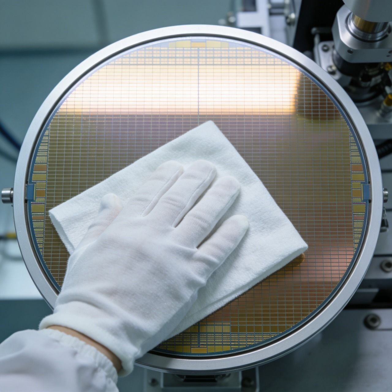
Ultra-Clean Process Wiping System for Semiconductor Manufacturing
| Process Step | Recommended Product | Key Technical Parameters | Application Scenario | Packaging Spec |
|---|---|---|---|---|
| Lithography Area Cleaning | BN.11040324 | 233.93% Abs., 18.7g Dry Wt., Ultra-low Ions | Reticle Cleaning, Lens Wiping, Scanner Interior | 10 pcs/bag, 100 bags/case |
| Post-CMP Cleaning | BN.11040218 | 254.25% Abs., 54.2g Dry Wt., Abrasion-Resistant | Post-polish wafer surface cleaning, Pad cleaning | Roll, 100m/roll |
| Ion Implantation Area | BN.11050805 | ESD Safe, 10⁶ Ω Surface Resistivity, Radiation-Resistant | Implanter chamber cleaning, Wafer transfer mechanism | 20 pcs/bag, 50 bags/case |
| Thin Film Deposition Area | BN.11050135 | Low Ionic Residue, NVR < 3 μg/cm² | CVD/PVD equipment cleaning, Reaction chamber maintenance | Custom Sizes, Packaging on Demand |
| Etch Process Area | BN.11051103 | Composite Structure, Acid/Alkali Resistant, 221.01% Abs. | Etch tool cleaning, Exhaust treatment system | 25 pcs/bag, 40 bags/case |
| Assembly & Test Area | BN.11050207 | Balanced Performance, 178.31% Abs., Cost-Effective | Mold cleaning, Test socket maintenance | 100 pcs/bag, 20 bags/case |
Company Partners


Reliable Guarantee Customer case feedback

4.9/5
Dr. Rachel Haldims
Solving a 5nm wafer defect problem
Surface charge decreased from 250V to <50V, and defect rate decreased from 12% to 1.8%.

5/5
Dr. Mariel Senry
Static electricity damage and lint can cause short circuits.
The electrostatic discharge (ESD) failure rate decreased from 8% to 0.6%, and the short circuit rate decreased from 5% to 0.3%.

4.8/5
Dr. Damian Pix
Optical equipment lens maintenance
No new scratches, charge maintained at <30V for over 8 hours, and imaging resolution improved by 15%.

4.5/5
Dr. Shi Yon
Wafer surface particulate contamination
The surface particulate contamination rate of wafers decreased by 70%, and the overall yield increased by 5%.
Microfiber cleanroom cloth
In the nanoscale world of semiconductor manufacturing, contamination control is not an option, but a necessity. Our microfiber cleanroom wipes, designed specifically for global semiconductor front-end manufacturing and precision back-end assembly, serve as a line of defense against particulate contamination, protecting sensitive circuitry and ensuring the highest product yields. Each wipe originates from our certified ISO Class 4 core production environment, manufactured and tested according to the most stringent IEST standards, and is committed to meeting the demanding requirements from mature processes to state-of-the-art packaging technologies such as 3D-ICs.
What makes your microfiber wipers specifically suitable for Class 1 and Class 10 cleanrooms in semiconductor fabs?
Our microfiber wipers are engineered for the most critical environments. The key is our continuous filament, 100% polyester microfiber construction which is inherently low-linting. Combined with our proprietary laser-sealing edge technology, we virtually eliminate edge shedding. Each batch is validated to release < 5 particles (>0.5µm) per square foot according to IEST-RP-CC004.3, making them ideal for photolithography, wafer inspection, and sensitive assembly areas.
We experience issues with solvent absorption and residue when cleaning precision parts. How does your product address this?
Our microfiber is designed for high absorbency with low NVR (Non-Volatile Residue). The split-fiber structure creates immense surface area to trap and retain contaminants and liquids within the fabric, rather than redepositing them. When used with high-purity solvents like IPA or acetone, our wipers consistently achieve NVR levels below 10 µg/ft² in standard tests. We recommend validating with your specific solvent in a controlled test.
Can you customize the size, packaging, and ESD properties of these microfiber wipers for our automated cleaning equipment?
- Size & Format: We can produce any roll dimensions, sheet size, or specialized die-cut shapes to fit your equipment.
- Packaging: Options include vacuum-sealed bags, clean PE pouches, or bulk packaging for automated dispensers, all in Class 100 cleanrooms.
- ESD Properties: We can embed permanent carbon-loaded fibers or apply topical treatments to achieve a consistent surface resistivity range from 10^6 to 10^9 ohms/sq, complete with full per-batch test data.
What is your quality assurance process, and can you support our audit and qualification requirements?
- Raw Material Control: Incoming fiber certification.
- In-process Checks: SPC (Statistical Process Control) on knitting, sewing, and cleaning.
- Final Batch Testing: Each batch is sampled and tested for particles, NVR, and ESD in our in-house lab. We provide full Certificate of Analysis (CoA) and Compliance (CoC).
We fully support customer audits (virtual or on-site) and provide all necessary documentation for your supplier qualification portal.