
Liquid Crystal Panel
Solution
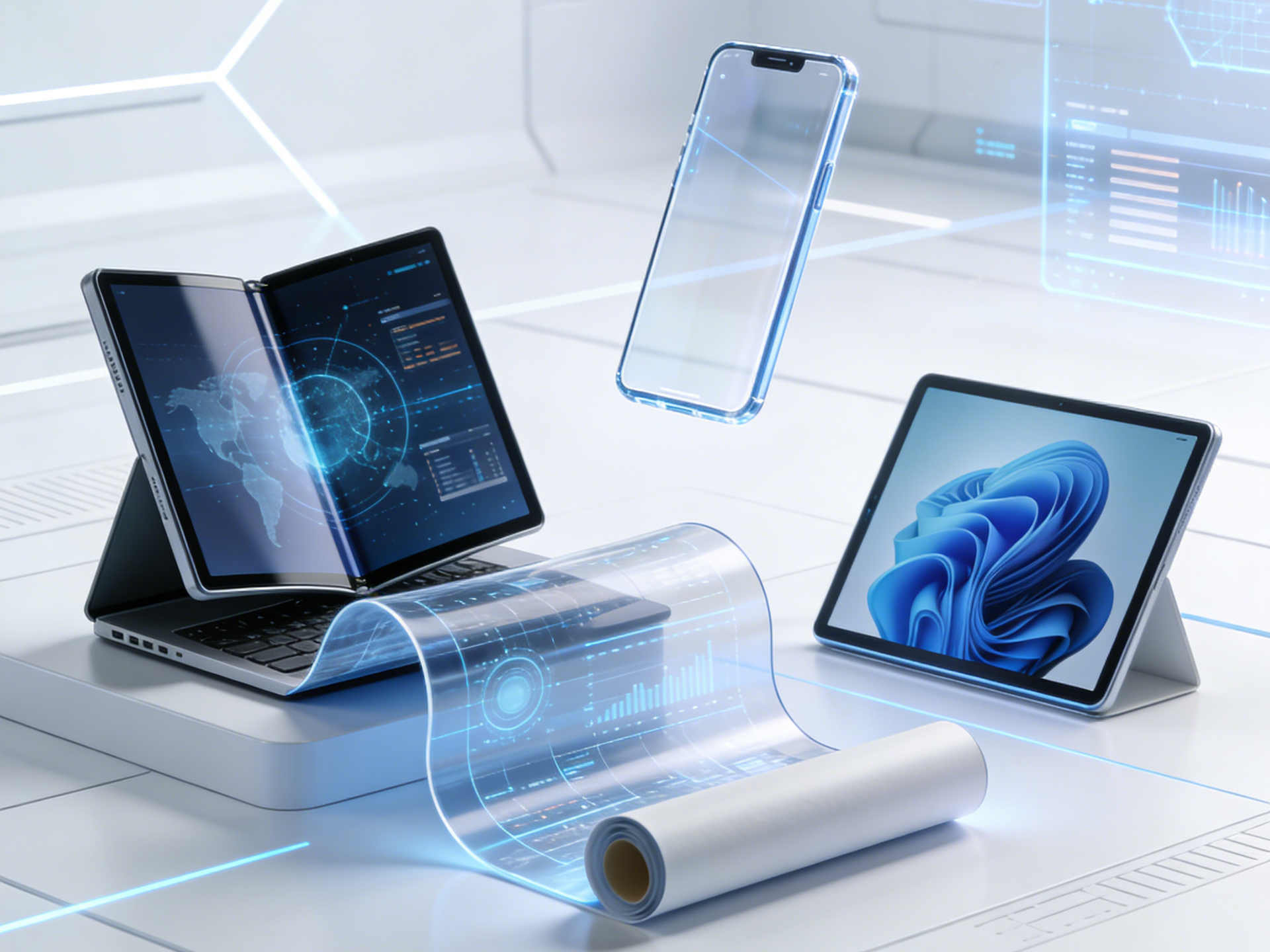
Precision Cleaning System for Display Panel Manufacturing, Providing Defect-Free Cleaning Assurance from G10.5 Gen Lines to Flexible OLED
5/5
bupclean
One-stop industry service
15 years experience
Liquid Crystal Panel (Display) Industry Solutions
| Process Step | Key Requirement | Recommended Product | Tech Parameters | Usage Standard |
|---|---|---|---|---|
| Glass Washing | Remove cutting dust, large particles | BN.11051103 | Composite, 221% Abs., Custom Sizes | 1 pc / G10.5 substrate |
| TFT Fabrication | Fine cleaning, Anti-static | BN.11050805 | ESD Safe, 159.84% Abs. | 300 pcs / 1000 wafers |
| Lithography Area | Ultra-clean, Low chemical residue | BN.11050135 | Low ionic residue, NVR<5μg/cm² | 5 pcs / 100 reticles |
| Post-etch | Acid/Alkali resistant, Residue removal | BN.11050422 | High wear resistance, Resists pH1-13 | 20 pcs / shift |
Cell Process Cleaning
Color Filter Formation: BN.11040324, ultra-soft, doesn’t damage RGB layers.
PI Coating: Recommend BN.11050201, low surface energy prevents adhesion.
Sealant Dispensing: Recommend BN.11050207, precise edge cleaning.
LC Dropping: Recommend BN.11040218, quickly absorbs overflow LC.
Module Process Cleaning
Polarizer Lamination: Recommend BN.11050202, medium absorption, good hand-feel.
TP Lamination: Recommend BN.11050137, durable type, cost-optimized.
Backlight Unit (BLU) Assembly: Recommend BN.11050312, high durability, dust removal.
Final Inspection: Recommend BN.11040324, ultra-clean, no streaks.
Company Partners


Reliable Guarantee Customer case feedback

4.9/5
Dr. Rachel Haldims
Solving a 5nm wafer defect problem
Surface charge decreased from 250V to <50V, and defect rate decreased from 12% to 1.8%.

5/5
Dr. Mariel Senry
Static electricity damage and lint can cause short circuits.
The electrostatic discharge (ESD) failure rate decreased from 8% to 0.6%, and the short circuit rate decreased from 5% to 0.3%.

4.8/5
Dr. Damian Pix
Optical equipment lens maintenance
No new scratches, charge maintained at <30V for over 8 hours, and imaging resolution improved by 15%.

4.5/5
Dr. Shi Yon
Wafer surface particulate contamination
The surface particulate contamination rate of wafers decreased by 70%, and the overall yield increased by 5%.
Liquid Crystal Panel Solution
In the micron and even nanometer world of display panel manufacturing, contamination control is not an option—it is a necessity. Our precision cleaning system for liquid crystal panels is specifically designed for front-end array processes and back-end module assembly, forming a critical defense line against particulate contamination. It protects sensitive circuitry and pixel structures, ensuring the highest product yields. Each cleaning solution originates from our ISO Class 4 core manufacturing environment, validated and tested according to the most stringent SEMI and display industry standards. We are committed to meeting demanding requirements ranging from mature a-Si processes to advanced LTPS, LTPO, and flexible OLED packaging technologies.
How is your precision cleaning system specifically suitable for defect-free requirements on G10.5 large substrates and flexible OLED lines?
Our cleaning system is engineered for the most critical cleanroom environments. The core technology lies in our megasonic resonance unit and ultra-low particle double-side brush structure, which achieves non‑contact cleaning with extremely low particle generation. Combined with our proprietary laminar‑flow high‑speed drying module, we virtually eliminate watermarks and re‑contamination. Each batch‑verified process, tested in accordance with IEST and SEMI standards, ensures that post‑clean surface particle counts (≥0.5 µm) are below 0.5 particles per cm². This makes our system ideal for photolithography, post‑etch cleaning, and pre‑evaporation surface preparation for flexible OLEDs, especially in photolithography, cell, and module bonding areas.
We experience issues with solvent residue and particle re‑deposition when cleaning precision panels. How does your system solve this?
Our cleaning system features high extraction efficiency and extremely low non‑volatile residue (NVR). The cavitation force of megasonics, combined with high‑pressure micro‑jetting, dislodges contaminants and chemical liquids from the substrate surface and promptly removes them, avoiding re‑attachment. When used with high‑purity deionized water or solvents such as IPA, the system consistently achieves post‑clean NVR levels below 15 µg/ft² (per standard test methods), with near‑zero residual particles. We recommend performing a full process validation on your specific panel process to achieve optimal parameter matching.
Can you customize the cleaning system for our special substrate sizes, throughput requirements, and ESD protection needs?
Dimensions & formats: We can provide customized chambers and transport rollers for non‑standard substrates ranging from G10.5 (2940 mm × 3370 mm) down to G4.5, as well as for flexible OLED roll‑to‑roll (R2R) lines of arbitrary web widths.
Throughput & integration: In‑line or off‑tool layouts are available; tact time can be optimized down to 30 seconds per sheet, and the system can be adapted to existing automated robotics and conveyor lines.
ESD protection: We can integrate permanent anti‑static ionizing bars and conductive roller materials within the cleaning module, achieving a consistent surface resistivity range of 106106 to 109109 ohms/sq. Full per‑batch ESD test data is provided, effectively protecting TFT circuits and OLED light‑emitting layers from electrostatic damage.
What is your quality assurance process, and can you support our audit and qualification requirements?
- Raw Material Control: Incoming fiber certification.
- In-process Checks: SPC (Statistical Process Control) on knitting, sewing, and cleaning.
- Final Batch Testing: Each batch is sampled and tested for particles, NVR, and ESD in our in-house lab. We provide full Certificate of Analysis (CoA) and Compliance (CoC).
We fully support customer audits (virtual or on-site) and provide all necessary documentation for your supplier qualification portal.