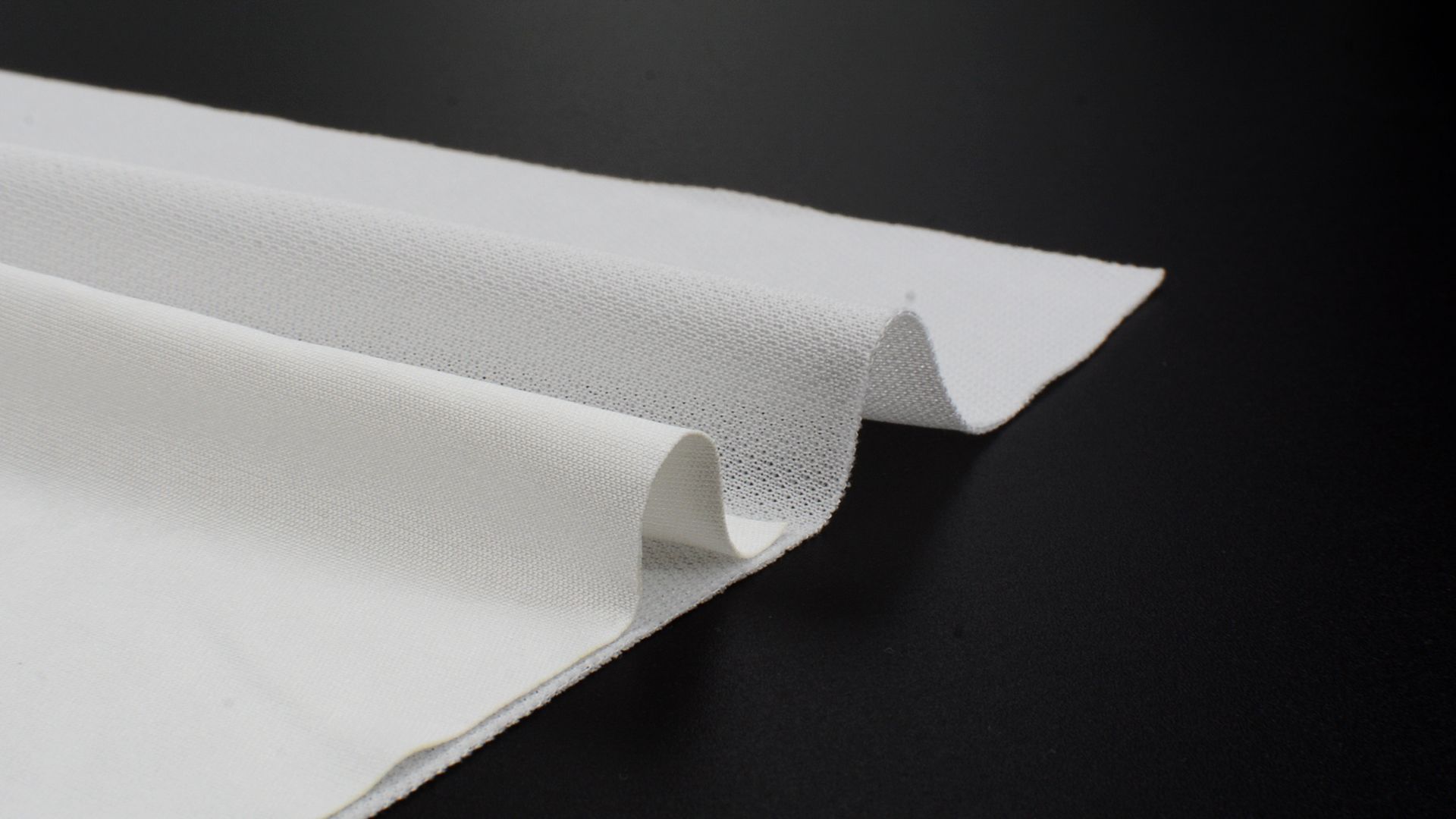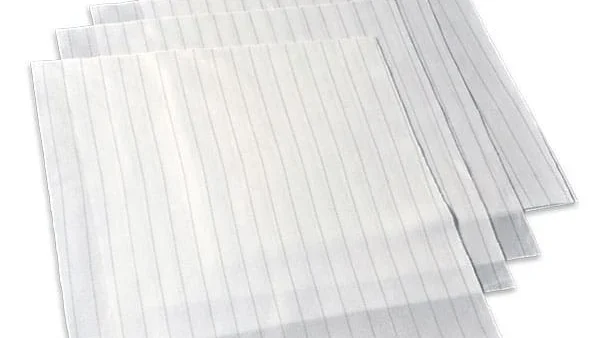
Photomasks and wafers are the most contamination‑sensitive surfaces in semiconductor fabrication. A single particle of 0.5 µm on a photomask can print a repeating defect across thousands of die. Standard wipes (even 180 g/m² ultrasonic) are not certified for sub‑micron cleanliness.
| Series | Part numbers | Grammage | Edge | Pack sizes | Particles (≥0.5 µm) | NVR (µg/cm²) |
|---|---|---|---|---|---|---|
| 3009 | BN.11040301/02/03 | 110 g/m² | laser | 100, 100, 400 | ≤3 | <5 |
| 3008 | BN.11020626/27, BN.23020605 | 110 g/m² | laser | 100, 100, 400 | ≤4 | <6 |
Detailed model breakdown
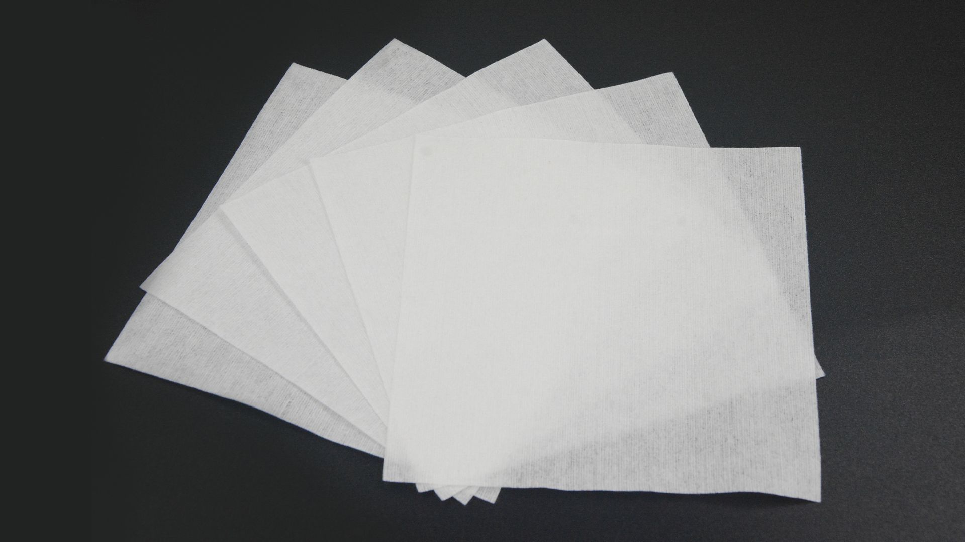
BN.11040301 – 9×9, 100 sheets/bag
Used for photomask cleaning stations. The laser edge creates a 1.2‑1.5 mm sealed zone. No loose fibers at the edge even after 10 wet‑dry cycles (tested for 50 mm travel). Metal ion content (ICP‑MS): Na 0.3 ppm, K 0.1 ppm, Fe <0.1 ppm, Cu <0.05 ppm, Cr <0.03 ppm. All below SEMI standard limits for Class 10 cleanrooms.
BN.11040302 – 6×6, 100 sheets/bag
Smaller size for wafer edge cleaning and reticle handling. Operators prefer this size because it fits inside cassette slots. In a 300 mm wafer fab, BN.11040302 reduced particle adders by 64% compared to the previous 9×9 wipe (operators were folding too much, creating creases that shed fibers).
BN.11040303 – 4×4, 400 sheets/bag
High‑pack version for automated wipe dispensers. Four hundred sheets per bag reduces bag changes by 75% vs 100‑sheet bags. Each sheet is individually folded for easy pick‑up. Used in brush box cleaning and nozzle tip wiping.
BN.11020626 (3008 series)
Alternative source for the same 110 g/m² spec. The difference is the base fabric supplier. Particle counts are slightly higher (≤4/cm²) but still within sub‑micron grade. Lower cost – about 12% less than 3009 series. Suitable for wafer handling tools and metrology stage cleaning.
| Parameter | BN.11040301 | BN.11020626 | Test method |
|---|---|---|---|
| Particle count (≥0.5 µm) | 2.8 /cm² | 3.9 /cm² | IEST‑RP‑CC004.3 |
| Particle count (≥5 µm) | 0.2 /cm² | 0.4 /cm² | IEST‑RP‑CC004.3 |
| Fibers (>100 µm) per 100 cm² | 0 | 1 | Microscopic scan |
| NVR (IPA extract) | 4.2 µg/cm² | 5.1 µg/cm² | gravimetric |
| Absorption capacity | 2.8× | 2.7× | internal method |
Application protocol for photomasks
Pre‑inspect the mask under UV light. Mark defect coordinates.
Use a new wipe (BN.11040301) for each mask. Never reuse.
Apply photomask cleaner (not standard IPA – IPA leaves residues). Dampen the wipe, not soak.
Wipe from center to edge in a single, continuous motion. No back‑and‑forth.
Discard immediately. Do not let the wipe dry on the mask.
Following this protocol, a mask shop reported 92% reduction in on‑tool particle defects after switching from a non‑certified 180 g/m² wipe.